
 Plico Team
1 min read
Can You Recycle Solar Panels?
Solar panels can be recycled in Australia if they are disposed of correctly. In most parts of the country, panels need to be disposed of as e-waste,...

Solar + Battery Rebates, Loans and Discounts available!
Find out what incentives you're eligible for and how much you could save.

Interest-free loan now available!
Find out if you're eligible for the NSW $15,000 intertest-free loan.

Solar + Battery Rebates, Loans and Discounts available!
Find out what incentives you're eligible for and how much you could save.
Interest-free loan now available!
Find out if you're eligible for the WA $10,000 intertest-free loan.
The three main types of solar panels are monocrystalline, polycrystalline and thin-film. Within these types are subgroups and variations of solar panels. All three solar panel types and their subgroups vary in efficiency, utility and manufacturing process.
There are various solar panel types that comprise the solar panel market; each has its own pros, cons, and discrepancies in performance. While in essence they perform the same task – harnessing the sun’s energy to power your home – their materials, manufacturing and end-of-life considerations differ. If you’re thinking about getting solar, you need to know which solar panel type is the best fit for you. Buckle in: we’re about to break down solar panel types, chemistry, and creation.
Monocrystalline solar panels derive their name from their manufacturing process. Each cell within a monocrystalline solar panel contains a thin wafer from a single silicon crystal.
The cell provides more space for the movement of electrons since it is composed of material from a single crystal. This leads to a better electrical flow and efficiency of solar power generation; monocrystalline solar panels are the most efficient solar panel type. However, because a monocrystalline solar panel comprises a single silicon crystal, there is high manufacturing wastage. This increased wastage is why monocrystalline is the most expensive solar panel type.
Polycrystalline solar panels are composed of silicon crystals. They get their name because they’re produced with multiple silicon crystals, unlike monocrystalline panels, which are created with a single silicon crystal. Polycrystalline solar panels use fragments from different silicon crystals. These fragments are gathered together and melted down. The molten crystals are then poured into a square mould, where they cool and solidify.
Polycrystalline solar panels are more affordable than monocrystalline panels because of their low wastage. However, because of their lower silicon purity, polycrystalline panels are less efficient and have a lower power capacity than monocrystalline solar panels. The higher the silicon purity of a material, the more adept it is at absorbing the sun’s heat. Polycrystalline solar panels also have a lower heat tolerance than monocrystalline solar panels and struggle to maintain efficiency in high-temperature environments.
The manufacturing process of monocrystalline and polycrystalline solar panels is similar, although the start of the process differs for each panel.
Monocrystalline solar panels use slices of single silicon crystal ingots. Silicon crystal ingots are most commonly made using the Czochralski method. In the Czochralski method, a seed crystal is placed in a vat of pure molten silicon at a high temperature. It is then pulled out while being rotated, and the molten silicon surrounds it to create one large crystal called an ingot.
Polycrystalline solar panels use slices from polycrystalline ingots. Polycrystalline ingots are made by melting shards of silicon crystals and pouring them into a mould until they cool and solidify.
Once the ingots are made and sliced, there are five stages to manufacturing crystalline solar panels. The five manufacturing stages are the texturing, diffusing, coating, printing and assembly of crystalline wafers.
Texturing is the first step in manufacturing a monocrystalline and polycrystalline solar panel. Texturing involves increasing the surface area of the silicon to allow for greater sunlight absorption. Next, corrosive chemicals are employed to remove a layer of silicon and leave the surface of the wafer etched with a series of irregular pyramid shapes. These irregular pyramid shapes bounce the sun’s rays around, increasing the energy the panel can extract from each sun ray.
The second step of manufacturing a monocrystalline and polycrystalline solar panel is diffusing. In solar panel manufacturing, diffusing involves giving electrical charge to the top or bottom wafers that act as semiconductors in a cell. The two primary methods of creating an electric field are the p-method and the n-method. Both involve doping one silicon wafer to create a difference in polarity to the other wafer. The swapping of electrons between the negatively charged and positively charged wafers creates the electrical field that generates solar power.
Coating the solar panel’s wafers is the third step in manufacturing a monocrystalline and polycrystalline solar panel. The wafer is coated with silicon nitride, which makes the surface less reflective and increases the amount of light it absorbs.
The fourth step of manufacturing a monocrystalline or polycrystalline solar panel is the process of printing. Printing involves laying a paste on the crystalline wafers. This paste is a metal conductor and helps the panel trap sunlight and create an electric field. Creating an electric field is how a solar panel generates solar power.
The final step of manufacturing monocrystalline or polycrystalline solar panels is assembly. Assembly entails soldering the solar cells into ribbons. Ribbons are typically ten cells long. Six ribbons are laid out to form a matrix containing sixty cells. This matrix is laminated onto an anti-reflective, tempered glass with a plastic back sheet. The final stage is placing the laminated matrix into a frame and fitting it with a junction box for electrical connections.
Passivated emitter and rear cell (PERC) panels are a variation of crystalline panels. They can use either monocrystalline or polycrystalline panels as their base, but they have an additional passivation layer on the rear surface of the cell. A passivation layer makes a solar panel more efficient through greater internal reflection, electron flow promotion, and high-wavelength light reflection.
Passivated emitter and rear cell (PERC) solar panels increase the internal reflection of sunlight. Increasing the internal reflection of sunlight boosts the amount of solar radiation absorbed by the cell. The greater the solar radiation a solar cell absorbs, the more solar power it will create. PERC solar panels increase this internal reflection by the passivating layer reflecting the light into the cell.
Another reason the efficiency of PERC solar panels is high is that a PERC cell enables greater electron flow and movement. Greater electron flow and movement create a stronger electrical current and more solar power.
Finally, PERC panels reflect high-wavelength light to prevent overheating the back sheet. Silicon wafers cannot absorb light over 1180 nanometres in wavelength, resulting in the light passing through the cell instead. When it passes through, it reaches the metal back sheet, where it is absorbed and increases the temperature of the back sheet. The passivation layers reflect the high wavelength light and stop the back sheet from overheating. This mitigates the risk of a decline in efficiency due to overheating.
Because a PERC solar panel improves the efficiency of the base crystalline panel types – monocrystalline and polycrystalline – a PERC monocrystalline solar panel will enhance the already efficient monocrystalline panel, as well as make it more expensive.
Bifacial solar panels are a variation of crystalline solar panels. Bifacial solar panels have solar cells on the front and back of their panels. Traditional solar panels are monofacial, meaning they only have cells on one side. Monofacial solar panels allow a portion of uncaptured sunlight to pass through and dissipate on their back panels. In contrast, bifacial solar panels are built of glass instead of an opaque material, allowing uncaptured and unmediated sunlight to pass through. This sunlight is reflected off the ground and captured by the back side of the bifacial solar panel. This increases the total energy capture. They are particularly useful around highly reflective surfaces. Most bifacial solar panels use monocrystalline bases but can also have a polycrystalline base.
Bifacial solar panels are less well known than other solar panel types as they aren’t particularly suited for residential roof mounting. The required frames for mounting a panel on a roof leave insufficient space between the panel and the roof. This severely limits the sunlight that reaches the back side of the panel. Between the space requirements and their higher cost, they are not a good choice for roof-based solar setups.
While unsuitable for a rooftop setup, they can still be useful for residential applications. Setting up bifacial solar panels on freestanding structures is a viable option for power generation. Carports and awnings are suitable for providing shade and a spot to produce energy.
A thin-film solar panel is a PV panel made of a thin piece of photovoltaic material embedded into either metal, glass or plastic. Many thin-film solar panels are flexible and don’t have frame backing. Because they don’t have a frame backing, thin-film panels are lighter than other solar panel types and are the easiest to install.
Thin-film solar panels are not limited by standardised sizing the way crystalline panels are and can be sized specifically for an individual’s needs. As a result, they’re less efficient than crystalline solar panels but more affordable. Thin-film solar panels struggle to cope with heavy weather, such as hail or extreme wind, because of their flexibility and thinness. The typical thin-film solar cell arrangement is a substrate, contact layer, photovoltaic layer, buffer and transparent conducting oxide (TCO).
The three types of thin-film solar panels are Cadmium Telluride (CdTe), Amorphous Silicon (a-Si) and Copper Indium Gallium Selenide (CIGS).
Photovoltaic layer: The thin-film layer responsible for absorbing light and converting it to electricity.
Substrate: A surface on which a thin film is applied. Substrates serve as backing or base layers for active photovoltaic components. They are made of materials such as glass, plastic or metal, depending on the requirements of the solar cells.
Transparent conducting oxide (TCO): An electrically conductive material with low light absorption. TCOs protect other layers, letting light into a solar cell and collecting the converted energy. TCOs are commonly made using combinations of indium, zinc and tin oxides.
Cadmium Sulphide (CdS): A commonly used buffer layer in certain thin-film cells. It is negatively charged to provide an opposing polarity to positively charged photovoltaic layers. CdS is highly transparent, allowing the most light possible to reach the photovoltaic layer below.
Contact layers: Tasked with carrying electrical current generated by the solar cell to the external load and back into the cell. Cells may have a back contact layer, a front contact layer or both depending on their structure. Contact layers are made of metal, most commonly molybdenum.
The first thin-film solar panel type is cadmium telluride (CdTe), which is manufactured using cadmium. It is a low-cost option with a small carbon footprint, minimal water requirements and low energy payback compared to all other solar panel types. CdTe thin-film panels can be made extremely thin. This makes them easier to apply and contributes to low manufacturing costs. CdTe produces a high efficiency level for capturing energy, particularly in low-light and high-temperature conditions. Unfortunately, CdTe panels are more expensive to recycle than other panels due to cadmium being toxic.
CdTe cells typically use glass as a substrate since it is cost-effective and adept at enduring various deposition processes. The CdTe layer is positively charged. It does the primary job of photovoltaic conversion and absorbs the most visible light shined on it. The CdS layer is placed on top of the CdTe layer and is negatively charged. These two layers work together to create the electric field that directs the electrical current. Techniques commonly used in the manufacturing of cadmium telluride thin-film panels are sputtering and electrodeposition.
The second thin-film solar panel type is amorphous silicon (a-Si). a-Si is manufactured using silicon, like crystalline panels, but remains shapeless. a-Si panels use considerably less silicon in manufacturing compared to crystalline solar panels. They are a low-cost option but prove inefficient compared to other solar panels. They are suited for uses that have low power requirements. Pure amorphous silicon has atomic bonding defects, so it must be alloyed with hydrogen (hydrogenated) to be effective in photovoltaic applications.
Two main factors affect the efficiency of a-Si thin-film panels. These are low structural homogeneity and the Staebler-Wronski effect. Low structural homogeneity refers to the uneven distribution of silicon in the amorphous layer. As a result, parts of the layer can be too thick or too thin, affecting absorption capacity. The Staebler-Wronski effect describes how unsaturated silicon atoms change their structure when exposed to light. This results in a decline in photovoltaic performance between 35% and 155%.
Amorphous silicon generates an electric field differently from other thin-film panels. It uses three layers of hydrogenated silicon. There is a positive layer, a negative layer, and a thicker intrinsic layer between the positive and negative layers. The intrinsic layer is responsible for photovoltaic absorption. The positive and negative layers of amorphous silicon create the electric field. Sputtering, chemical vapour deposition and PECVD are the most commonly used techniques to deposit a-Si thin-film.
The third thin-film solar panel type is copper indium gallium selenide (CIGS). CIGS are manufactured using thin layers of copper, indium, gallium and selenium deposited on a backing made of glass or plastic. Their efficiency is the highest among thin-film solar panels due to the materials used in the combination. However, they are still less efficient than crystalline silicon panels. CIGs are considered extremely versatile. They can be manufactured using several different processes and work with various substrates.
Glass, plastic and aluminium foil have been used as suitable substrates for CIGS thin-film panels. The CIGS layer is responsible for photovoltaic absorption. It is positively charged. The CdS layer sits on top of the CIGs layer and is negatively charged. Together, these two layers make an electric field. Common deposition methods used in manufacturing CIGS include sputtering, evaporation, electrochemical, and ion-beam deposition.
Thin-film panels are manufactured using deposition. Deposition refers to the process of applying a thin film to a surface. Physical deposition processes alter a substance’s form but not its chemical makeup. Chemical deposition processes alter the chemical makeup of the substance being deposited. There are six most commonly used deposition processes in thin-film manufacturing. These are evaporation, sputtering, chemical vapour deposition, plasma-enhanced chemical vapour deposition, electrochemical deposition and ion beam deposition.
The six most common deposition methods in thin-film manufacturing are:
The manufacture of solar panels comes with certain human rights concerns. Polysilicon is an essential component in solar panel manufacturing. Much of the mining of polysilicon occurs in the northwest Xinjiang region of China. Human rights organisations have criticised this region for the inhumane treatment and detention of the Uyghur people. In addition, there are reports of slave labour employed in producing solar panel components.
Plico takes these inhumane manufacturing procedures seriously. This is why the company chooses to partner with technological manufacturers who have a history of high-level corporate responsibility and operates under an ethical framework as we do.
Solar panels provide a more sustainable and ethical energy source than fossil fuels. However, issues can arise regarding solar panel waste. Most residential solar panels last between 25 and 30 years. They are recyclable, but the process can be complicated. Additionally, many companies forgo recycling the panels to save money. Mandates exist in Europe to ensure companies recycle old solar panels; however, this is not the case in the United States. This results in high wastage from America. As solar panels grow in popularity, waste will increase if mandates are not in place.
Plico is committed to environmental sustainability for the entire life cycle of our solar panel and battery systems. As up to 95% of the materials in a solar panel can be recycled, our goal is to ensure as much of this is redirected from landfill as possible. We work with various recycling companies to reuse or recycle solar panels removed for new installations. Additionally, we’re committed to recycling the panels we install when they are at the end of their productive life, and we’re working with the first Australian company to develop a solar battery recycling program.
You can mix different types of solar panels in a solar array. However, voltage and currents vary between different types of solar panels. These discrepancies lead to lower overall power output. Therefore, using panels with similar voltages and amperages is recommended if mixing different types of solar panels.
Different types of solar panels can be mixed in two ways: in series or parallel. Mixing solar panels in series creates a single flow of current. This results in the power capacities of the panels adding up to a sum total. If one panel has a lower power output than the other panels, they will each provide that lower power output. Marrying panels in series results in a higher voltage. Combining solar panels in parallel splits the flow of electric current. This allows the panels to function with increased independence. One panel with a lower power output won’t lower the power output of other panels. Mixing panels in parallel results in a higher amperage; the inverter’s capacity determines the maximum voltage and amperage. Combining solar panels in parallel leads to better power output.
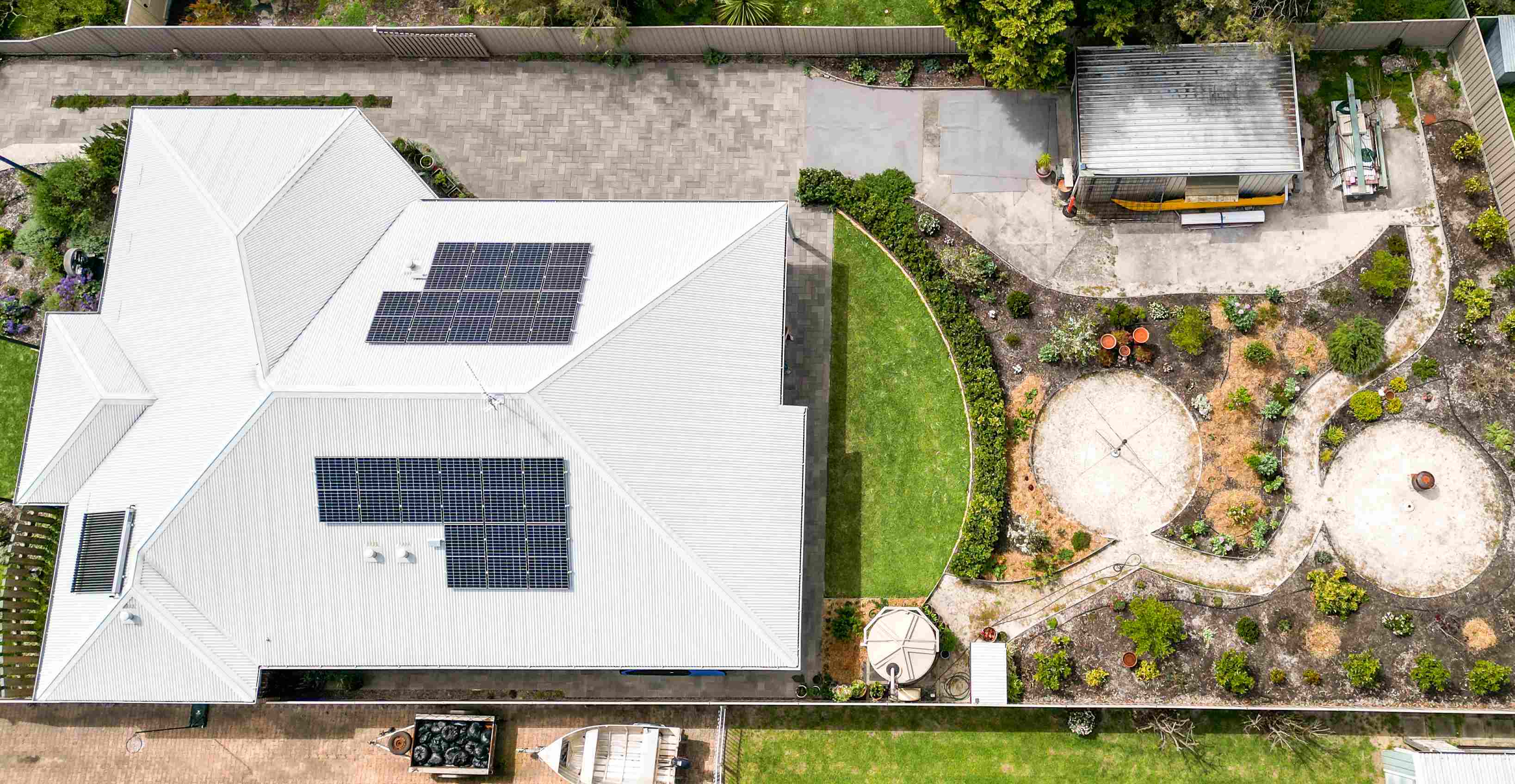
Plico’s solar + battery systems use various high-quality panels that provide value and performance for our members.
Plico is a technologically agnostic company, meaning that we are continuously evaluating the best equipment on the market to ensure our systems are delivering industry-leading performance while being affordable for our members. That’s why our systems have monocrystalline solar panels, the most efficient solar panel type.
If you’re looking to make the switch to solar, excited to save money on your electricity bills and kick harmful coal, fill out the form below.
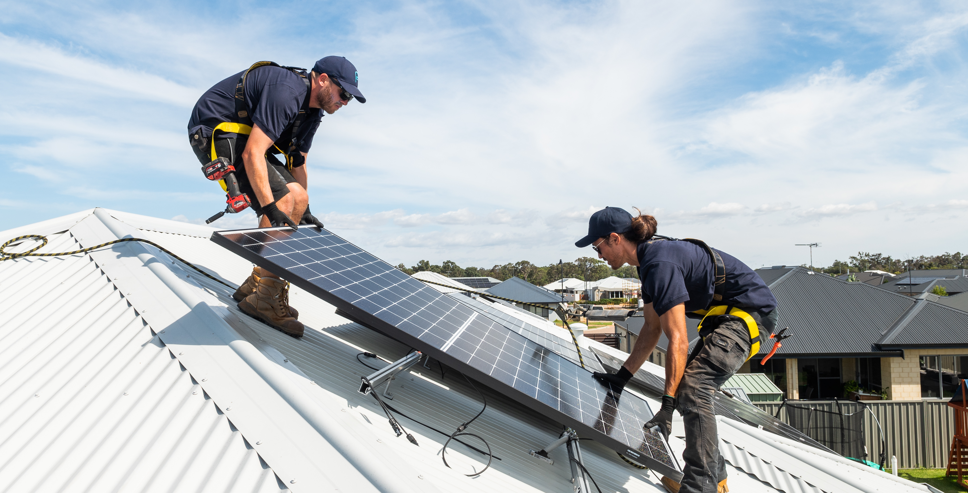
Alternatively, you can chat with one of the switched-on Plico team members on 1300 175 426. The best part? You won’t have to pay any big upfront costs, and we provide ongoing support for the duration of your time with us.
1 min read
Solar panels can be recycled in Australia if they are disposed of correctly. In most parts of the country, panels need to be disposed of as e-waste,...

1 min read
Understanding Solar Panel Efficiency Solar panels convert sunlight into electricity. This is known as the photovoltaic (PV) effect, which is why...
1 min read
The best orientation for solar panels in Australia is north, between a 30 to 45-degree tilt, with location deciding the best angle within this range....